OUR RESEARCH
Programmable Spacing Multiplication in Optical Frequency Combs
Optical frequency combs have gained wide applications in optical arbitrary waveform generation, optical spectroscopy, optical communications, and so on. It is always challenging to generate wide-spaced, broadband, and flexibly tunable frequency combs due to limited bandwidth of the RF source and electrical components. Our group has demonstrated a method for wide-spaced comb generation initiated with a relatively low-rate optical pulse train. This scheme involves two main processes. First, the repetition rate of an incident optical pulse train is multiplied with high energy efficiency through the temporal Talbot effect. Next, the rate-multiplied optical pump pulses are used to modulate a co-propagated CW probe via the ultrafast cross-phase modulation (XPM) effect in a highly nonlinear fiber (HNLF). Consequently, an optical frequency comb is generated around the CW probe with a programmable comb spacing determined by the pump pulse rate.
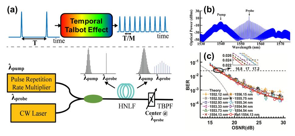
Fig. 1. (a) Schematic illustration on the generation of spacing-multiplied optical frequency combs. (b) Experimentally generated comb around the probe and the broadened pump spectrum. (c) System performance of 32 GBaud 16-QAM data modulation on 11 selected optical carriers from the frequency comb.
To enrich the flexibility of comb space multiplication, our group introduced a method based on modulation-assisted temporal Talbot effect and XPM. Specially designed electrical patterns are utilized to periodically modulate the phase of the incident optical pulses. After the temporal Talbot effect, the pulse rate can be multiplied by a factor determined by the phase modulation patterns. Therefore, programmable control on the pulse rate can be achieved by modifying the electrical modulation patterns. Subsequently, the variable-rate pump pulses interact with the CW probe light via XPM, giving rise to optical combs with tunable spacing. This scheme provides an energy-efficient method to achieve flexible control on comb spacing by using both the linear and nonlinear properties of optical fibers while relying on relatively low-speed electronic devices and circuits.
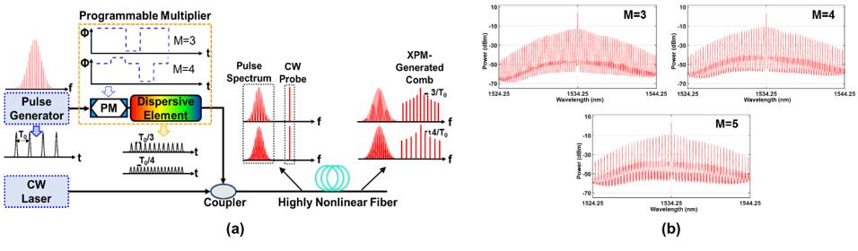
Fig. 2. (a) Principle of programmable comb spacing multiplication. PM: phase modulator. (b) Experimentally measured optical frequency combs with variable multiplication factors.
[1] B. Zheng, Q. Xie and C. Shu, “Comb spacing multiplication enabled widely spaced flexible frequency comb generation,” IEEE/OSA J. Lightwave Technol., vol. 36, no. 13, pp. 2651-2659 (2018).
[2] Q. Xie, B. Zheng and C. Shu, “Wide-spaced optical frequency comb with programmable spacing,” IEEE Photon. Technol. Lett., vol. 30, no. 10, pp. 975-978 (2018).
Microwave Photonic Signal Processing with Gain-Transparent Stimulated Brillouin Scattering
Gain-transparent stimulated Brillouin scattering (SBS) is a unique process in an optical fiber in which the Brillouin pump and Brillouin Stokes wave act simultaneously on a counter-propagating optical signal. The pump and Stokes wave are located at offset frequencies from the signal with a center frequency. The Brillouin pump will generate a gain profile over a frequency range centered at the Brillouin frequency downshift, while the Brillouin Stokes wave will generate a loss profile over a frequency range centered at the Brillouin frequency upshift. The real parts of the Brillouin gain and loss will cancel out while the imaginary parts will add up to induce a strong phase shift within a narrow bandwidth around the signal.
Our group proposed and demonstrated the application of gain-transparent SBS in microwave photonic subsystems. We developed a method to generate microwave waveforms with tunable temporal profiles and repetition rates based on gain-transparent SBS together with chromatic dispersion introduced by a dispersion compensating fiber (DCF).
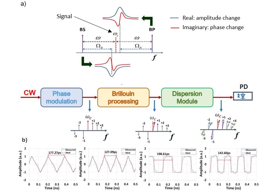
Fig. 1. (a) Principle of gain-transparent SBS in an optical fiber. BP: Brillouin pump; BS: Brillouin Stokes wave. (b) Schematic illustration of microwave waveform generation by gain-transparent SBS. (c) Generated triangular and rectangular waveforms with different repetition rates.
We also utilized gain-transparent SBS to mitigate the power fading effect caused by chromatic dispersion in analog photonic links. A significant improvement has been demonstrated in the linearity of the links. In addition, the scheme offers the flexibility for the system to operate at different transmission lengths.
.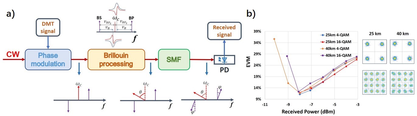
Fig. 2. (a) Proposed scheme of an analog photonic link. (b) Error vector magnitude (EVM) against received power for discrete multitone (DMT) data transmission over the links. Inset shows the constellation diagrams at the lowest EVMs of the two links.
[1] J. Liu, C. Huang, and C. Shu, “Photonically assisted microwave waveform generation by gain-transparent SBS-induced carrier processing,” Optics Letters, vol. 42, no. 19, pp. 3852-3855 (2017).
[2] J. Liu, X. Wu, C. Huang, H. K. Tsang, and C. Shu, “Compensation of Dispersion-Induced Power Fading in Analog Photonic Links by Gain-Transparent SBS,” IEEE Photonics Technology Letters, vol. 30, no. 8, pp. 688-691 (2018).
Raman-Assisted Optical parametric processing for High Speed Coherent Communication Systems
Raman-assisted optical parametric processing combines the Kerr effect and Raman effect in a silica-based highly nonlinear fiber, aiming to deliver high-performance nonlinear processing for high-speed coherent communication.
We build a coherent communication platform to investigate the applicability of Raman-assisted optical parametric processing. Digital signal processing algorithms are developed to handle the physical layer impairments including optical fiber chromatic dispersion, polarization demultiplexing, laser frequency and phase offsets, and phase noise. We design block-wise carrier-phase recovery in the framework of variational Bayesian Kalman filter as shown in Fig. 1. The algorithm can recursively track the measurement noise to optimally estimate the carrier evolution [1].
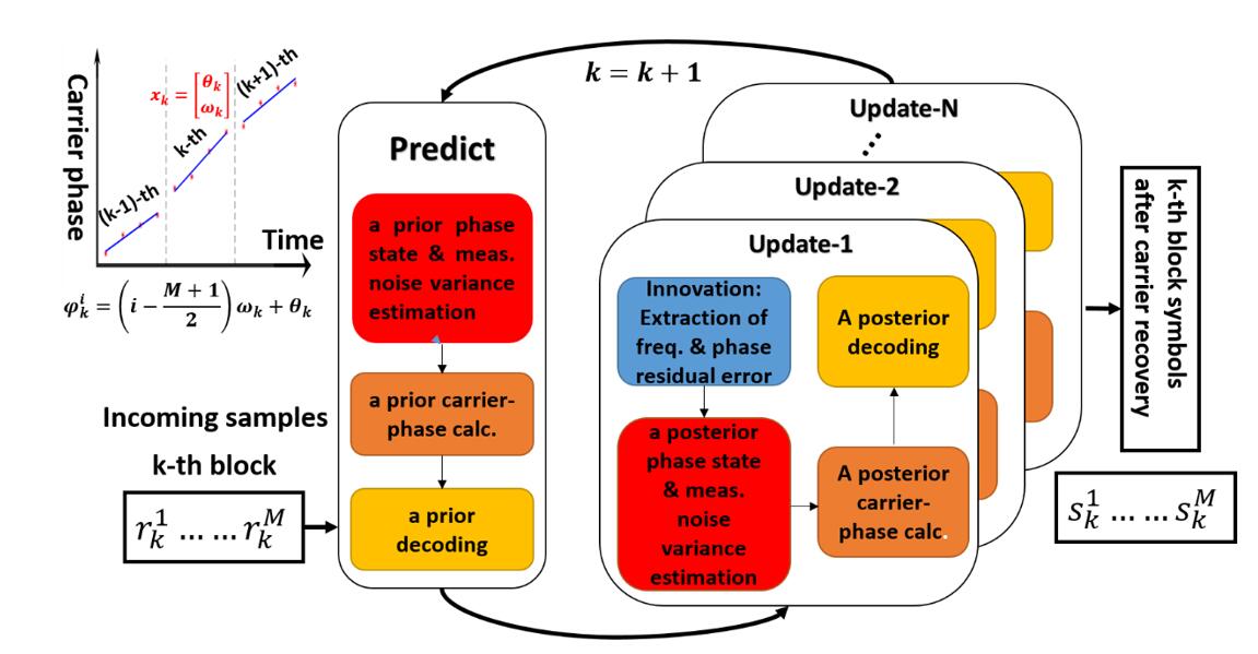
Fig.1 Schematic diagram for the block adaptive carrier-phase recovery scheme.
Raman-assisted parametric optical amplifiers are investigated for improved linear amplification. By explicitly tracing the full electrical field of each spectral component, we rigorously identify that the evolution of phase relation among the signal, pump and idler can compensate the gain reduction caused by pump depletion, leading to the deferred presence of gain saturation. Experimentally, both the static characterization using a continuous-wave probe and dynamic characterization using a Nyquist-shaped 16-QAM signal validate the enhancement of the dynamic range. Fig. 2 shows the dynamic characterization in terms of the Q-factor variation and the constellation changing. Raman-assisted parametric optical amplifiers demonstrate the potential on parametric amplification of data signals in higher-order modulation formats [2].
Phase-sensitive nature of the parametric process has been exploited to combat with nonlinear distortion in data transmission. Here, an optical add-drop filter enabled by Raman-assisted phase-sensitive amplification (RA-PSA) is proposed, which can be an essential subsystem for data routing in optical links with in-line phase-sensitive amplifiers. The presence of Raman pump can augment the nonlinear interaction among the signal, parametric pump and idler to achieve a low-crosstalk add-drop filter. Fig. 3 shows performance comparison between the conventional PSA and RA-PSA using the bit error rate (BER) measurement of a 16-QAM signal [3].
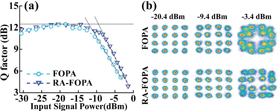
Fig. 2. Dynamic characterization using a 16-QAM signal. (a) measured Q-factor versus average input signal power; (b) constellation diagrams of output from fiber optical parametric amplifier (FOPA) (top) and Raman-assisted (RA)-FOPA (bottom) for input power at -20.4 dBm, -9.4 dBm and -3.4 dBm, respectively.
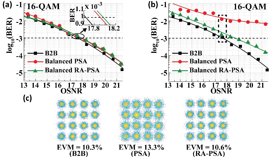
Fig. 3. BER measurement using signals in 16-QAM format for (a) drop filter, (b) wavelength reuse of the central channel (Ch2) at the signal band. (c) Constellation diagrams of B2B, balanced PSA and balanced RA-PSA in wavelength reuse. The corresponding BER points are indicated in (b) using the dashed rectangular boxes.
[1] B. Zheng and C. Shu, “Block carrier-phase recovery with recursive noise adaptive Kalman filtering for 16-QAM signals,” Proc. of OECC/PS, Paper TuB2.4, (2016).
[2] B. Zheng, X. Fu, and C. Shu, “Dynamic range improvement in fiber optical parametric amplifier with Raman pumping,” IEEE Photon. Technol. Lett., vol. 30, no. 12, pp. 1159-1162, (2018).
Digital Signal Processing Techniques Assisted Distributed Brillouin Optical Time Domain Analyzer Fiber Sensor
Distributed optical fiber sensors based on Brillouin optical time domain analyzer (BOTDA) sensors have attracted both academic and industrial interest. To enhance the performance of BOTDA, many technologies have been successfully applied. Our group has proposed to improve the performance of BOTDA through the use of digital signal processing (DSP) techniques.
Firstly, BOTDA assisted by support vector machine (SVM) for ultrafast temperature extraction is proposed and experimentally demonstrated. The temperature extraction is treated as a supervised classification problem. The Brillouin gain spectrum (BGS) serving as feature vectors are classified into different temperature classes by the SVM models trained using ideal BGS curves with different temperatures, linewidths and shape factors. In addition to a better accuracy compared with traditional curve fitting methods, the processing speed for temperature extraction using SVM is ~100 times faster than that using conventional curve fitting. Apart from the conventional BOTDA, we have verified that SVM can also be used to extract temperature information in differential pulse-width pair BOTDA (DPP-BOTDA).
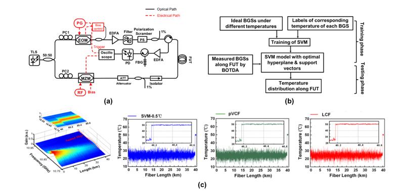
Fig. 1. (a) Experimental setup of BOTDA. (b) Procedure of SVM for temperature extraction in BOTDA. (c) Measured BGS distribution along 40.6 km FUT with last 400 m section heated and temperature distribution along FUT extracted by SVM-0.5℃, pseudo-Vigot curve fitting (PVCF) and Lorentzian curve fitting (LCF).
BOTDA performance is limited by noise, which causes inaccuracy in measurements. The conventional method of denoising BOTDA signals is ensemble averaging, despite that averaging thousands of BOTDA traces to obtain an acceptable SNR is very time consuming. Image denoising such as wavelet denoising (WD) and non-local means (NLM) have attracted lots of recent attention as the techniques would not add any hardware complexity. Our group has analyzed the performances of BOTDA sensors assisted by WD and NLM techniques in terms of measurement accuracy and spatial resolution for the first time and we proposed and experimentally demonstrated an advanced image denoising techniques, i.e. block-matching and 3D filtering (BM3D) to denoise the BOTDA data with the least error of measurement accuracy and spatial resolution compared with WD and NLM.
.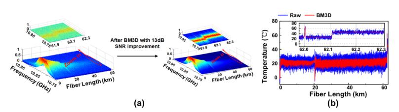
Fig. 2. (a) Measured BGS distribution along FUT and after BM3D denoising with 13dB SNR improvement. (b) Corresponding temperature distribution along FUT with measured data and after BM3D denoising.
[1] H. Wu, L. Wang, N. Guo, C. Shu and C. Lu, “Brillouin optical time-domain analyzer assisted by support vector machine for ultrafast temperature extraction,” IEEE/OSA J. Lightwave Technol., vol. 35, no. 19, pp. 4159-4167 (2017).
[2] H. Wu, L. Wang, Z. Zhao, C. Shu and C. Lu, “Support vector machine based differential pulse-width pair Brillouin optical time domain analyzer,” IEEE Photonics Journal, vol. 10, no. 4, 6802911 (2018).
[3] H. Wu, L. Wang, N. Guo, C. Shu and C. Lu, “Support vector machine assisted BOTDA utilizing combined Brillouin gain and phase information for enhanced sensing accuracy,” Optics Express, vol. 25, no. 25, pp. 31210-31220 (2017).
[4] H. Wu, L. Wang, Z. Zhao, N. Guo, C. Shu and C. Lu, “Brillouin optical time domain analyzer sensors assisted by advanced image denoising techniques,” Optics Express, vol. 25, no. 5, pp. 5126-5139 (2018).
Raman-Enhanced Multichannel Optical Parametric Signal Processing
With the increasing demand of communication bandwidth, the manipulation and characterization of ultrafast data signals using optical parametric approach based on four wave mixing (FWM) has attracted much interest. Time lens processing that relies on space-time duality provides the capability to transform high-speed serial data into parallel channels that can be detected by lower speed receivers. Meanwhile, in multichannel optical parametric sampling, the pulsed pump defines a time window to sample multiple channels simultaneously. Raman amplification can be advantageously applied to improve the power uniformity in serial-to-parallel conversion and to mitigate the signal crosstalk in multichannel optical sampling.
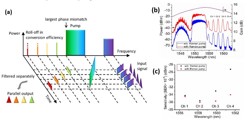
Fig. 1. (a) Principle of Raman assisted FWM in time lens based serial-to-parallel data conversion. The Raman gain peak is located at the pump wavelength at which the corresponding phase mismatch is the largest. (b) Spectral output after the serial-to-parallel data conversion. The violet curve shows the Raman gain profile. (c) Measured receiver sensitivities of the four channels with and without Raman pump.
We have demonstrated a scheme to enhance the uniformity of conversion efficiency in serial-to-parallel data conversion via time lens processing. In our approach, Raman amplification is applied to enhance four-wave mixing in a highly nonlinear fiber. By carefully selecting the pump wavelength, the Raman gain profile can be exploited to compensate the roll-off in conversion efficiency resulting from the increasing phase mismatch between the linearly chirped pump and the signal. Improvement in receiver sensitivity is demonstrated and the sensitivity variation across the output channels is reduced.
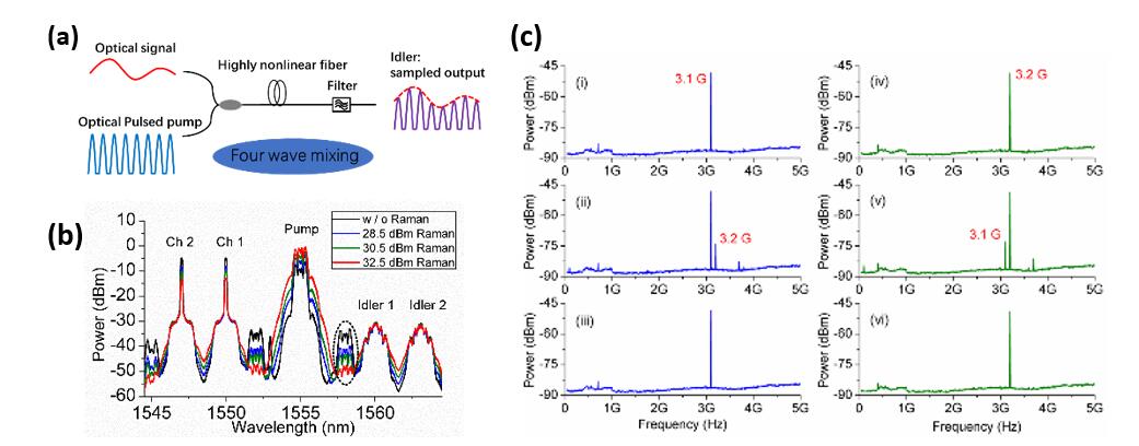
Fig. 2. (a) Parametric sampling based on four wave mixing. (b) Measured optical spectrum at the HNLF output. Dotted area indicates one of the spurious mixing products. (c) Measured electrical spectra of Idler 1 (left) and Idler 2 (right).
Owing to the wide Raman gain bandwidth, the signal, parametric pump, and idler can be simultaneously amplified during the FWM process. Thus, the conversion efficiency is improved. Also, the fluctuation of the conversion efficiency is reduced since the depletion of the parametric pump is compensated by Raman amplification. We propose and demonstrate an optical technique to mitigate the crosstalk in multichannel optical parametric sampling via backward Raman amplification. The performance is improved through the benefits of compensating for parametric pump depletion and enhancing the conversion efficiency. The input signal power is reduced but the output idler power can be maintained. Consequently, the spurious FWM products and the crosstalk induced frequency components are suppressed.
[1] J. Ru, Q. Xie, C. Huang, B. Zheng, and C. Shu, “Enhanced performance in serial-to-parallel data conversion via Raman-assisted time lens processing,” Opt. Lett., vol. 42, no. 10, pp. 1939-1942 (2017).
[2] J. Ru, C. Huang, and C. Shu, “Crosstalk Mitigation in Multichannel Optical Parametric Sampling via Raman Amplification,” IEEE Photon. Technol. Lett., vol. 29, no. 24, pp. 2272-2275 (2017).
Optical carrier regeneration and its application in self-coherent communication systems
In an optical receiver circuit, self-coherent detection can be realized using a phase-locked optical carrier. The detection scheme offers the advantage of simple process for equalization, unlike heterodyne detection where frequency and phase estimation is required to retrieve the signal. The locked carrier can be obtained from two common carrier regeneration techniques, namely, optical injection locking (OIL) and stimulated Brillouin scattering (SBS). The regeneration thus plays a key role in both conventional homodyne detection and recently proposed Kramers-Kronig (KK) detection systems.
Our group proposed a novel scheme for realizing KK detection by digitally inserting two weak pilot tones at the shorter wavelength side of the data signal at the transmitter. The tones are spectrally separated by the fiber Brillouin frequency shift. At the receiver, the pilot tone farther away from the signal spectrum is filtered out as a pump seed for optical injection locking. The amplified pump then transfers its energy through SBS to the virtual carrier, which is the pilot tone near the signal.
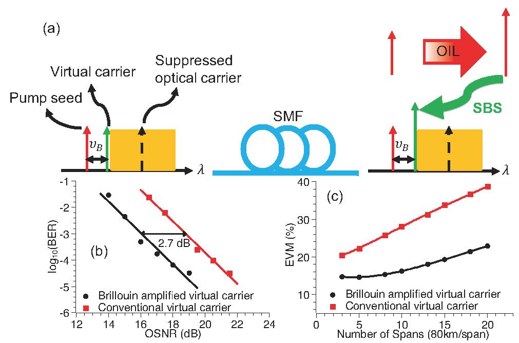
Fig. 1. (a) Conceptual diagram of Brillouin amplified optical carrier applied for KK detection scheme. (b) Experimental result on BER against OSNR after an 80-km transmission. (c) Simulation result on EVM against the number of fiber transmission spans
We further demonstrated that an optical carrier can be extracted from a signal generated with a blockwise phase-switching (BPS) technique for the purpose of locking the optical frequency combs at the transmitter and the receiver in a wavelength division multiplexing (WDM) system. At the transmitter, all optical carriers in the frequency comb are modulated with conventional coherent signals, except for the central carrier which is modulated by the BPS signal. After fiber transmission, a portion of the BPS signal is tapped out for OIL- or SBS- assisted carrier regeneration before the direction detection is performed. Therefore, a locked frequency comb seeded by the regenerated carrier can be produced at the receiver. The frequency comb thus provides a bank of local oscillators (LOs) for self-coherent detection of other data channels.
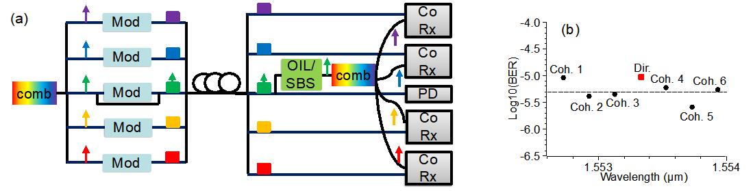
Fig. 2. (a) Conceptual diagram of the proposed comb-based WDM system. (b) BER of all channels after 80 km transmission.
[1] Q. Zhang, B. Zheng and C. Shu, “Kramers–Kronig detection with Brillouin-amplified virtual carrier,” Opt. Lett., vol. 43, no. 6, pp.1367-1370 (2018).
[2] Q. Zhang and C. Shu, “Carrier regeneration from a blockwise phase- switching signal for a frequency comb-based WDM system,” Opt. Lett., vol. 43, no. 15, pp.3694-3697 (2018).
Optical Signal Processing Techniques Based on Four-Wave-Mixing Bragg Scattering
Four-wave-mixing Bragg scattering (FWM-BS) can realize different functions such as signal replication, unitary transform, frequency up-conversion or down-conversion. In particular, FWM-BS with several different frequency spacings can be applied for multiple signal replications to different wavelengths. Thus, wavelength multicast can be achieved, which is a promising functional block in future dynamic all-optical networks. To obtain a uniform performance in wavelength multicast, the phase matching condition needs to be well satisfied for all the generated channels. The condition can be fulfilled by precisely engineering the dispersion of the nonlinear medium. Alternatively, we propose dynamical control of the phase matching condition in FWM-BS processes using gain-transparent stimulated Brillouin scattering (SBS). Flexible control of the system is thus realized. In general, the phase mismatch in both the red-shifted and the blue-shifted multicast channels increases with the frequency spacing. By applying gain-transparent SBS, a phase shift is added to the FWM pump carrier such that the phase mismatch can be alleviated. Consequently, the conversion efficiency of the multicast channels will be balanced.
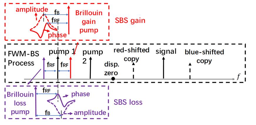
Fig. 1. Schematic illustration on dynamic control of phase matching in the FWM-BS process.
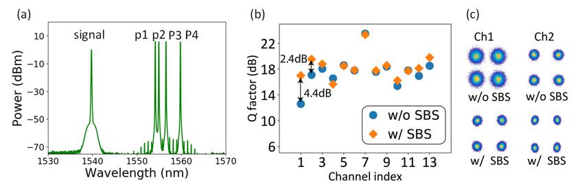
Fig. 2. (a) Optical spectrum of the signal and pumps input. (b) Q factor of the generated channels. (c) Constellation diagrams of channel 1 and 2 with and without applying gain transparent SBS.
Apart from wavelength multicasting, FWM-BS can be utilized to realize high-speed tunable optical delay line. Conventional slow-light based tunable delay suffers from intrinsic speed limits incurred by the thermal-optic or acousto-optic effect. Nevertheless, by exploiting the unitary transformation property of FWM-BS, we can achieve tunable phase amplification. Thus, high-speed delay tuning can be achieved by controlling the amount of Kerr effect, which itself has a response time in the femtosecond range.
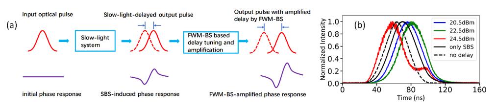
Fig. 3. (a) Principle of high-speed delay amplification using FWM-BS. (b) Experimentally measured optical delay with fixed SBS pump power and variable FWM pump power.
[1] N. Zhang, J. Liu, C. Huang, and C. Shu, "Enhanced performance of wavelength multicasting by gain-transparent stimulated Brillouin scattering," IEEE Photon. Technol. Lett., vol. 30, no. 6, pp. 585-588 (2018).
[2] N. Zhang, L. Fu, J. Liu, and C. Shu, "Surpassing the tuning speed limit of slow-light based tunable optical delay via four-wave-mixing Bragg scattering," Opt. Lett., vol. 43, no. 17, pp. 4212-4215 (2018).
High-Speed Graphene-on-Silicon Nitride Waveguide Photodetectors
Conventional III–V compound and germanium (Ge)-based photodetectors have been well developed and widely used commercially. Nevertheless, dense integration of the devices with complementary metal–oxide semiconductor (CMOS)-compatible materials is still challenging due to the demanding integration technology and high cost. Our group investigates the integration of CVD monolayer graphene onto a Silicon Nitride waveguide and use a metal-graphene junction to enhance the optical field for effective photodetection.
By arranging the electrode in a GND–Signal–GND (G–S–G) structure [Fig. 1(a)], we obtain an intrinsic responsivity of ∼15 mA/W under zero bias at a wavelength of 1550 nm with an electro-optic bandwidth of ∼30 GHz. This is the first study of a Si3N4 waveguide-integrated CVD graphene photodetector that simultaneously demonstrates high-speed and high responsivity. The performance is comparable to those of the best photodetectors prepared with pristine graphene, which however can hardly be adopted for large scale production.
.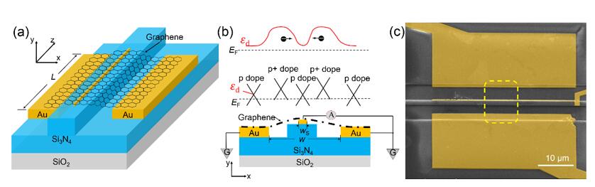
Fig. 1. Schematic of the device. (a) Schematic of the photodetector with a length of L. (b) Top: band diagram of the photodetector at zero bias. Fermi level, EF, is represented by the dotted line, and the Dirac energy position, εd, is represented by the solid curve. Bottom: cross-section of the device with a signal electrode of width of wS and channel width w. (c) Scanning electron microscope (SEM) image of a photodetector (sample A with L = 40 μm, wS ≈ 70 nm). The metal contacts are colored for clarity.
Graphene photodetectors have attracted research attention because of their potential high speed and broad spectral bandwidth. However, their low responsivity and quantum efficiency compared with germanium or III–V material based photodetectors limit their practical use. Our group has demonstrated a chemical vapor deposited graphene photodetector integrated on a silicon nitride waveguide with interdigital metal contacts. The channel spacing is reduced down to 200 nm. At zero bias, a metal-graphene junction is used for photodetection, which is beneficial for an electro-optic bandwidth of 33 GHz in the 1550 nm wavelength band. At a bias of 1V, a photoconductive responsivity of 2.36 A/W at 1550 nm was observed. The high speed and high responsivity make the device promising for photodetection in the telecommunication window. A diffusion model is applied to study the carrier transport in the graphene channel. By adopting this model, the high performance of the device is well explained. The main limitation in the responsivity of graphene photodetectors is also analyzed.
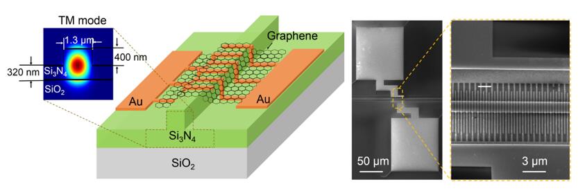
Fig. 2. (a) Schematic of a graphene-on-Si3N4 waveguide photodetector with transverse-magnetic (TM) mode distribution. (b) SEM image of a fabricated photodetector before graphene transfer.
[1] Y. Gao, G. Zhou, N. Zhao, H. K. Tsang, and C. Shu, “High-performance chemical vapor deposited graphene-on-silicon nitride waveguide photodetectors,” in Opt. Lett., vol. 43, no. 6, pp. 1399-1402 (2018).
[2] Y. Gao, L. Tao, H. K. Tsang, and C. Shu, “Graphene-on-silicon nitride waveguide photodetector with interdigital contacts," in Appl. Phys. Lett., vol. 112, 211107 (2018).
Optical Phase Conjugator for Nonlinear Distortion Mitigation in Fiber Transmission Links
Optical phase conjugation (OPC) offers an effective means to compensate for fiber dispersion and nonlinearity in transmission links. The processing approach enjoys the benefits of wide optical bandwidth, multi-wavelength operation, and transparency in bit rate and modulation format. Potential advantages also include reduction in power consumption, cost, and latency. Our recent study shows that by applying backward Raman amplification to fiber-based OPC, the undesirable nonlinear noise can be substantially suppressed. Consequently, improvement in both the optimum launched power and the Q factor are experimentally observed in a multi-wavelength coherent optical OFDM communication system [1].
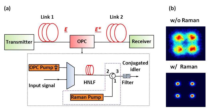
Fig. 1. (a) Experimental setup for Raman amplification enhanced OPC module and (b) corresponding constellation diagrams.
Furthermore, OPC can also be adopted for direct detection transmission links. In particular, Kramers-Kronig (KK) receiver-based optical transmission has gained increasing popularity due to the greatly simplified receiver structure compared to a conventional coherent receiver. KK detection is commonly designed to operate in short-span transmission systems. Recent analysis shows that it is also capable for use in long-haul transmission. Therefore, it is crucial to identify an effective way to compensate for both dispersion and nonlinear distortion in such links. In this project, we investigate the performance enhancement of KK receiver-based transmission links by applying OPC to mitigate the signal degradation. Compared to pure digital signal processing approach, higher bandwidth and faster processing speed can be achieved.
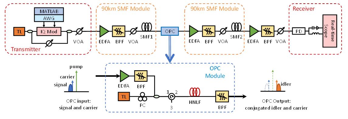
Fig. 2. Experiment on KK direct detection system with extended transmission distance using OPC.
[1] C. Huang and C. Shu, “Raman-enhanced optical phase conjugator in WDM transmission systems,” Optics Express, vol. 26, no. 8, pp. 10274-10281 (2018).