1. Draw schematic, (Pspice MicroSIM)
Check your Design !!
2. Draw PCB, (PADS PowerPCB)
Defining board size, pad and line shapes,
1 mil = 1/1000th of an inch, 50 mil = 0.05", assuming 0.8mm drill size.
or check it in workshop !!
Print a positive UV translucent film. (Need 2 Films)
Print it by Laser printers. The Film is for laser printing !!!
The printer setting is at least 600dpi resolution.
It is very important that the printer produces a good solid black with no toner pinholes.
Always check the solid line on your film. (Need 2 Films)
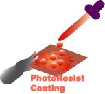
3. Coating Positive PhotoResist (PR) on PCB
Clean PCB by cleanser, dry carefully avoiding all grease/oil. 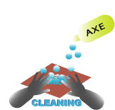
(VERY IMPORTANT for ARTWORK)
Dry the PCB about 20 minutes at 80oC before coating PR.
Avoiding get dust settling on the wet resist.
Coating photoresist (Red colour) thickness uniform. (NOT so THICK)
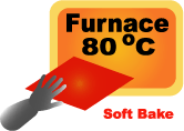
4. Drying Furnace (Bake)
Drying photoresist about 20 minutes at 80oC. (NOT so hot !!)
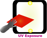
5. UV Exposure
Exposed to ultra-violet light using a UV exposure BLACK BOX.
DONT see the UV lamp !! it Cause eye and skin damage !
Switches on the UV lamps before 3-5 minutes of UV exposure.
PCB is sandwiched between two light sources to expose both sides.
Expose a PCB in about 10 minutes. Overexposure is better than underexposure.
6. Develop PR
Develop the PR by using Developer mixture about 1-3 minutes.
The mixture is about 1 part developer to 5 parts water.

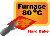
7. Drying Furnace (HARD Bake) or REDO =)
If the pattern is OK, then Drying photoresist about 20 minutes at 120oC.
Otherwise, REDO it !! =)
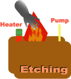
8. Etching
Ferric Chloride etchant is used. It is is dark yellow.
Dissolved etchant in warm water about 30-40oC until no more will dissolve.
It will damage eyes and anything - use gloves and safety glasses and wash off any skin splashes immediately.
It attacks ANY metal including stainless steel, so use a plastic container or glass baker.
IMMERSE PCB IN heated bubble-etch tank with pump and heater,
a PCB will etch in well under 10-15 minutes. (UNTIL ETCH ALL EXPOSED COPPER)
Check your pattern !!
9. Cleaning
Ferric Chloride etchant will damage anything, so clean PCB, container, table with WATER immediately.
REMOVE PhotoResist by ACETONE, then Alcohol and WATER !!
10. Drill holes
Typical hole sizes for ICs and resistors is about 0.8mm.
DO it in WORKSHOP. USE safety glasses !!
11. Soldering
USE safety glasses !!
All joint parts must be clean.
Clean the tip of the hot soldering iron on sponge.
Heat the joint with the iron for under a second.
Continue heating, then apply sufficient solder to form ball on the joint.
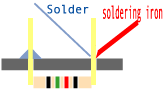
Remove the iron.
Takes 3-4 seconds to solder the joint.
Do not move parts until the solder has cooled.
USE desoldering pump to Remove the solder from a joint !!